A conversation on exactly how China is special from various other nations in PCB Assembly. China is currently called the most heartland for electronic devices producing. Actually, more than 80% of the electronic items worldwide are manufactured in China. Now, you may ask why is the whole PCB setting up treatment in the USA a lot various from others. Well, to start with, the entire procedure below is pretty much similar to that of China.However, in the USA
, the actions associated with PCB Setting up is a little different than China's through-hole and also surface area place process. There are a number of factors for this distinction. Allow us look at a few of them.The primary distinction remains in the method of add-on of the elements to the COMPUTER board. The Chinese typically favor through-hole as well as surface area install where the parts are installed using silk seam or heat-set glue. The COMPUTER boards are soldered with each other utilizing numerous cords as well as ports. The components are simply soldered together via the holes. This technique does not call for any soldering whatsoever as well as therefore is called "wire solder"or"warm soldering ". It is as a result more cost-efficient. Second of all, the technique of attachment of components to
the board is different in China contrasted to that of the USA. When the elements are stuck to the COMPUTER board through-hole or surface mount approaches, they are usually hot firm or glued. The parts are normally iron-soldered or hot-soldered. This makes it difficult for the welder to utilize solder paste stencils. solder paste patterns are a conventional method that makes it really simple to solder the components to the board. An additional advantage of utilizing solder paste stencils is that it removes the need for soldering the COMPUTER board.Thirdly, the method of COMPUTER board manufacture differs in China from that of the USA.
The PC manufacturing process which includes laying out sheets of circuit boards onto a strong substrate is called"reflow soldering". PCBs are made with reflow-soldering in the following manner. A stencil is first utilized to draw the design of the PCB, and afterwards several similar pcb's are set out utilizing parallel tabs.The PCB maker prepares the COMPUTER board according to the specification offered by the customer. They make adjustments as
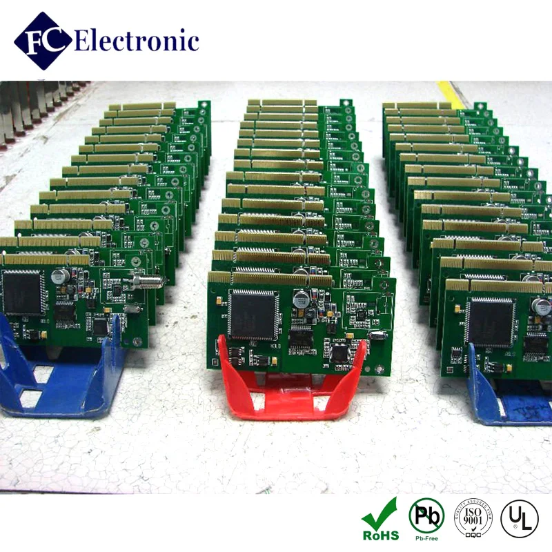
per the customer's requirements and include elements as required. The last PCB assembly is then created with the aid of UV treating tools. The published circuit card are then packaged in appropriate packaging materials such as sleeves or containers. They are then shipped to the clients. "Layered through-holes "are one more type of published circuit board assembly. They are formed by etching a location in which components can be fitted.
Etched components are frequently the case with the PC board production process. PC layered through-holes are popular with circuit card of different sizes and features.The COMPUTER board production approaches are based upon three standard concepts: hot air plating, cold air as well as wave soldering. Hot-air plating involves spraying a circuit onto the surface of
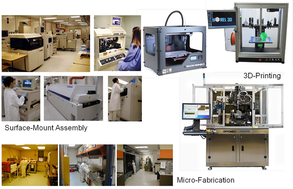
the web utilizing an application tool. The warm air fuse melts the exposed circuit elements. The PC board setting up is then put in a soldering equipment which thaws the solder and also fastens the parts. PCB assembly with solder soldering techniques is called "efficient conductive solder joint setting up ". This kind of setting up procedure happens inside the manufacturing facility where digital devices are produced. The job platform is a squeegee to push or an automated pallet racking machine. Elements are fed with a hose pipe into the receptacle at very high pressures. The hose pipe is then by hand launched so that the clamps holding the elements can pull them with each other. This is done at routine intervals in order to ensure that the entire assembly process occurs smoothly.PCBS assessment is the following step of the manufacturing board examination process. Throughout this phase, a top quality examiner completely takes a look at the condition of the components being used in manufacturing. The assessors seek defects and also wear and tear in the boards. They additionally look for the visibility of shrinkage,
bending, dampness transfer as well as dampness storage.Identification of the manufacturing mistake can be done by executing multidimensional testing. This consists of but is not restricted to the problem discovery. This step validates that the error did not low volume PCB Assembly happen throughout the original screening of the product or procedure. It is throughout the multidimensional testing that the electrical qualities of the final product are examined.
This is done one element at a time. This is carried out in order to recognize the one side mixed assembly which might only have actually taken place during the hand-operated screening process.